
Project
A moving average, built in hardware
Inside a VHDL signal filter: the four-sample datapath, ROM handshake, reset controllers, and simulation checks on a DE2-115 FPGA.
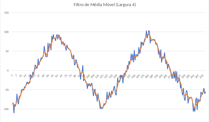
A moving average only takes a few lines of arithmetic. Putting it on an FPGA means answering several other questions: which samples are available on this clock cycle, when should memory be written, and what happens when someone presses reset halfway through? Most of this project sits around the addition and division.
I implemented the datapath, controllers, and board interface in 2022 for Laboratório de Sistemas Digitais at the University of Aveiro. The project was submitted with Luíz Fernando. It runs on a Terasic DE2-115: a 256 × 8-bit ROM supplies a noisy triangular signal, a four-sample filter smooths it, and a RAM of the same size stores the output. The board displays both values as signed decimal numbers.
Following the signal through the circuit
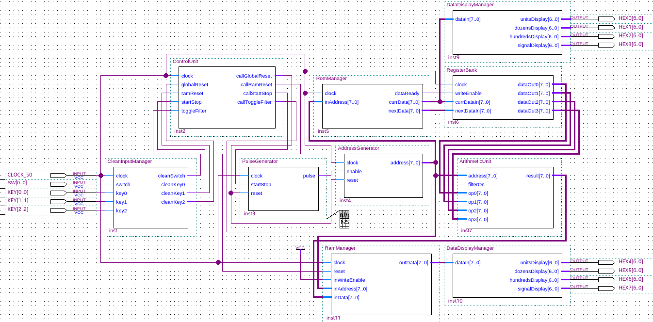
The address generator supplies the sample position to the ROM manager, arithmetic unit, and RAM manager. The ROM manager fetches two values; the register bank combines them with two retained values; the arithmetic unit selects their average or the current sample. Its result goes to RAM at the current address.
The display paths branch off separately. One shows the current ROM sample, while the other reads the stored RAM value. Input conditioning and the main controller decide when addresses advance, when memory clears, and whether filtering is enabled.
Everything clocked uses CLOCK_50, the board’s 50 MHz clock. PulseGenerator produces an enable roughly every half-second, giving the displays a readable pace. It does not create a second clock. Both memories are described in VHDL inside the FPGA design; the signal does not come from an ADC or the board’s external SDRAM.
Keeping four samples in the right places
The filter averages four samples: the two before the current address, the current sample, and the one after it.
y[n] = (x[n-2] + x[n-1] + x[n] + x[n+1]) / 4The x[n+1] term shaped the register bank. Shifting previously read values can supply history, but it cannot supply a future value. I added separate inputs for the current and following ROM samples.
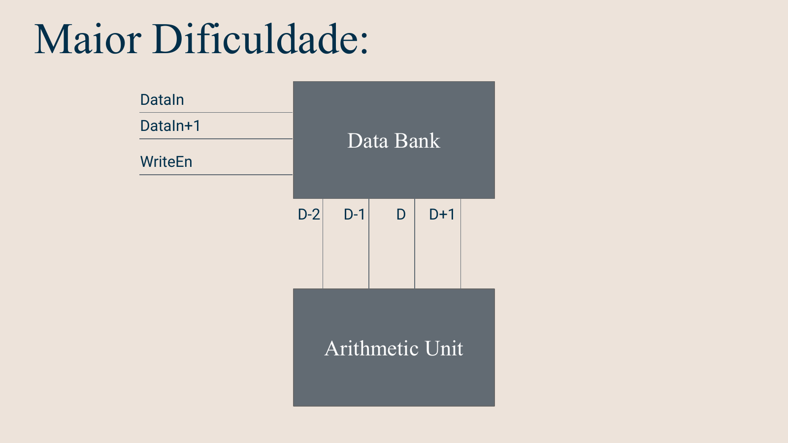
Inside the bank, s_Data0 holds the current value, s_Data1 the previous value, s_Data2 the one before that, and s_Data3 the lookahead. On a rising edge with write-enable asserted, the assignments are:
s_Data2 <= s_Data1;
s_Data1 <= s_Data0;
s_Data0 <= currDataIn;
s_Data3 <= nextDataIn;
These assignments take effect together. s_Data1 receives the old current sample, while s_Data2 receives the old previous sample. The ROM contains the entire input, so the next sample is available to fetch; a live input would require one sample of waiting.
Fetching the pair before shifting the bank
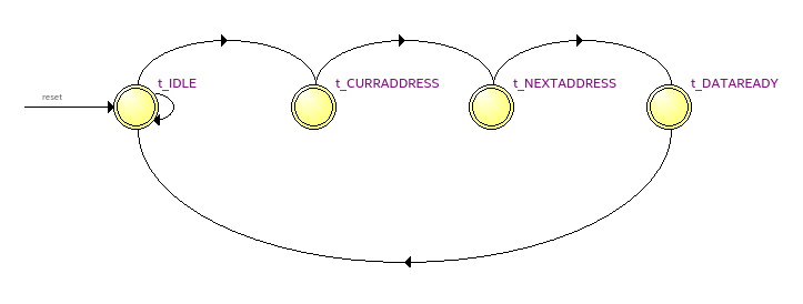
The ROM read is combinational, but RomManager sequences the two addresses over clock edges. It remembers the last requested address and starts a fetch when the input changes. The state names alone do not quite describe when each value is captured:
| Edge | ROM manager action |
|---|---|
| 1 | In t_IDLE, detect the changed address and move to t_CURRADDRESS. |
| 2 | Select ROM address n; move to t_NEXTADDRESS. |
| 3 | Capture x[n], select n+1, and move to t_DATAREADY. |
| 4 | Capture x[n+1], raise dataReady, and return to t_IDLE. |
| 5 | Lower dataReady; the register bank consumes its previous high value and loads the pair. |
That last edge matters. Both processes run on the same clock, so the bank sees the ready signal from before the edge. It does not load the lookahead on the edge that first asserts ready. In the top level, s_DataReady connects directly to the bank’s writeEnable, making each completed fetch one history update.
Signed arithmetic and the ends of the signal
ArithmeticUnit converts each operand to a signed integer before summing. Four signed eight-bit values can total between −512 and 508; their average still fits in eight bits. Integer division truncates toward zero, then TO_SIGNED(..., 8) converts the result back.
At address 2, the values are -87, -83, -110, and -87. Their average is -91.75, so the hardware stores -91. This also means a replacement using an arithmetic right shift would need care: negative values do not necessarily round the same way.
Addresses 0, 1, and 255 bypass the average because their windows extend outside the stored signal. Switching the filter off selects the same passthrough path everywhere. Although the eight-bit address counter wraps after 255, the averaging window does not wrap. The first two bypassed samples also allow the bank’s history to fill before address 2 is filtered.
The interactive version uses all 256 original ROM samples and these arithmetic and boundary rules. Move through the addresses or switch filtering off to inspect a window. It illustrates the calculation, not the FPGA’s memory or clock timing.
256 samples · signed 8-bit values
The original ROM signal, one sample at a time.
Address 2 · Filter enabled
(-87 + -83 + -110 + -87) ÷ 4 = -91.75 → -91
Two previous samples, the current sample and the following sample. Integer division drops the fractional part toward zero.
Resetting memory without losing the position
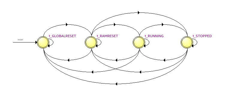
Startup passes through global reset and RAM reset before entering t_RUNNING. The global reset holds the main sample address at zero. RAM reset then writes zeroes across memory, using a separate eight-bit counter inside RamManager:
s_WriteEnable <= '1';
s_Address <= STD_LOGIC_VECTOR(s_AddressReset);
s_DataIn <= "00000000";
s_AddressReset <= s_AddressReset + 1;
The controller holds the clearing state long enough to visit all 256 locations. Because this counter is independent of the sample address, a RAM-only reset can preserve the current position. keepRunningState records whether to resume or remain stopped afterwards. A global reset instead returns to zero and resumes processing.
Normal writes take a different path: the manager registers the sample address and arithmetic result, and the RAM writes those registered inputs on the following edge. The RAM’s read output follows the selected address without another clocked read stage.
Controls that make the result visible
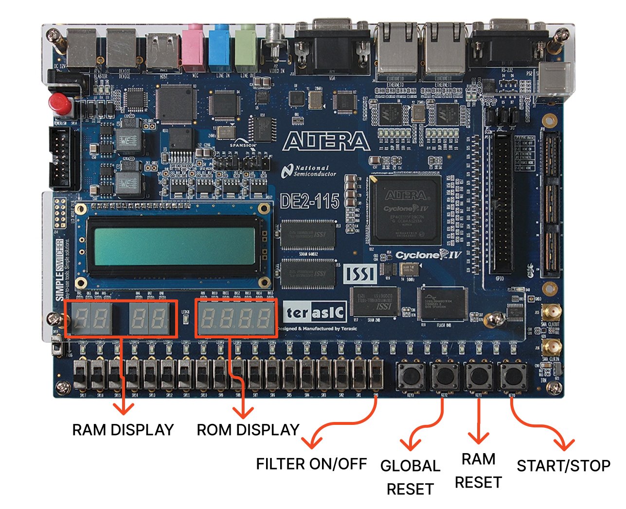
SW[0] selects filtering or bypass. KEY[0] pauses or resumes, KEY[1] clears RAM, and KEY[2] requests global reset. The active-low buttons pass through a 100 ms debounce interval and generate one event per qualified press. The filter switch is sampled on the system clock.
Pausing controls address advancement, while the top-level RAM write-enable remains tied to '1'. The current location continues receiving the arithmetic output, so changing the filter switch while paused lets you compare raw and averaged values at the same address. After a RAM clear, that location is written again even if processing remains stopped.
Checking the arithmetic and the timing
I used component simulations for the address generator, register bank, and arithmetic unit. The original captures show the signals being inspected.



The repository’s Python script applies the same window to the ROM data and prints all 256 raw/filtered pairs. Its decimal results provide a separate arithmetic reference. The VHDL benches supply stimulus for waveform inspection; they do not contain automated pass/fail assertions.
The first change I would make is an explicit result-valid signal for RAM writes. Currently a new address can briefly receive an old result while the ROM fetch is in progress, before being overwritten with the settled average. The half-second demonstration interval leaves ample time, but does not replace that handoff.
Reset and pause also deserve system-level assertions. The pulse generator retains its output while stopped, so stopping exactly when the enable is high is an edge case; its reset is checked only while running, so global reset does not guarantee a fresh half-second timer phase. These interactions sit beyond the archived component checks. The 50 MHz clock and readable demonstration rate are design settings, not a measured maximum throughput.
The repository includes the complete Quartus project, VHDL modules, testbenches, and Python reference. The original report preserves the diagrams and simulation captures shown here.